NAND
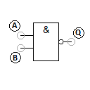
The output Q is only set to 0 if all inputs (A, B) have the value 1. The function of a NAND gate corresponds to that of an AND gate, whereby the output level is inverted by a NOT gate.
Truth table
| A | B | Q |
|---|---|---|
| 0 | 0 | 1 |
| 0 | 1 | 1 |
| 1 | 0 | 1 |
| 1 | 1 | 0 |
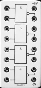
The IC 74HC00 is used as a component in the training package TP 1012 from Festo Didactic.
Adjustable parameters
| Designation | Range | Default value |
|---|---|---|
| Voltage level (lo) | 0.1 ... 24 V | 0.8 |
| Voltage level (hi) | 0.1 ... 24 V | 2 |
| Designation | Range | Default value |
|---|---|---|
| Voltage level (lo) | 0 ... 24 V | 0 |
| Voltage level (hi) | 0.1 ... 24 V | 5 |
| Resistance | 0.1 ... 1000 Ohm | 40 |